2025.08.08 Friday
How Sputtering Could Drive the Adoption of High-Performance ScAlN-Based Transistors
Researchers unveil the critical role of growth temperature in sputter epitaxy of scandium aluminum nitride films on gallium-nitride heterostructures

Gallium nitride (GaN)-based high electron mobility transistors (HEMTs) are a type of field-effect transistors (FETs) designed to operate at very high frequencies with low noise. As such, they have been widely applied in high-power and high-frequency applications, like high-speed wireless communications, power switching devices, and power amplifiers. HEMTs utilize a heterojunction, which is a junction between two different semiconductor materials, typically GaN and aluminum GaN (AlGaN). This junction creates a narrow region called the two-dimensional electron gas (2DEG), where electrons have very high mobility, resulting in excellent high-frequency performance.
Scandium aluminum nitride (ScAlN) has attracted significant attention as a novel barrier material that can further enhance the performance of GaN HEMTs. It exhibits large polarization, which increases electron densities in the 2DEG. Additionally, its ferroelectric nature makes it suitable for use as a ferroelectric gate material in ferroelectric HEMTs. Such a gate enables dynamic control over the 2DEG, offering potential to diversify the functionality of GaN-based devices. Conventional methods to grow ScAlN layers on GaN require complex techniques and high processing temperatures. In contrast, sputtering is a promising alternative, offering a minimal setup with the possibility of low-temperature processing. However, studies on sputtering-based growth of ScAlN on GaN remain limited, and the influence of growth temperature on its electrical and structural properties remains unclear.
In a new study, a research team led by Associate Professor Atsushi Kobayashi from the Department of Materials Science and Technology at Tokyo University of Science (TUS), Japan, successfully grew ScAlN thin films on AlGaN/GaN heterostructures using sputtering and studied the effect of growth temperature on their properties. "Compared to expensive and complex deposition techniques, sputtering, widely used in electronics manufacturing, can enable the mass production of ScAlN thin films at much lower costs, making high-performance devices more accessible," explains Dr. Kobayashi. The team also included Mr. Shunsuke Ota, a 2024 graduate of TUS. Their study was published in the journal APL Materials on August 7th, 2025.
The researchers epitaxially grew ScAlN films with 10% scandium content on AlGaN/AlN/GaN heterostructures through sputtering at varying temperatures. They then studied the structure of the films using atomic force microscopy (AFM) and high-energy electron diffraction. Their analysis revealed that epitaxial growth was achieved even at a low temperature of 250 °C, and surface flatness of the films improved with increasing temperature. Notably, a clear step-and-terrace surface structure was observed for the sample grown at 750 °C, indicating high structural quality.
Hall-effect measurements revealed that the carrier density in the 2DEG for the sample grown at 750 °C reached 1.1 × 1013 cm−2, approximately three times that of AlGaN/AlN/GaN heterostructures without ScAlN. In contrast, films grown at lower temperatures exhibited lower carrier densities than those of the initial non-ScAlN heterostructures. These results demonstrate that growth temperature is critical for 2DEG formation within the heterostructure. The improvement in carrier density at 750 °C was attributed to improved structural quality. However, the electron mobility in all ScAlN samples was reduced, compared to the initial heterostructure, likely due to the roughness and structural imperfections introduced by the ScAlN barrier near the AlGaN/AlN/GaN interfaces.
"The findings of this study highlight the key role of growth conditions in the sputter epitaxy of ScAlN films," highlights Dr. Kobayashi. "Importantly, our study demonstrates the viability of sputtering for growing high-quality ScAlN layers on GaN, offering a practical path towards the commercialization of high-performance GaN HEMTs with ScAlN barriers. This will lead to the widespread use of these transistors, which are fundamental to the development of highly efficient, energy-saving devices that can operate under harsh conditions, including electric vehicles and space vehicles, leading to the development of a sustainable future."
We hope that Dr. Kobayashi's research can lead to large-scale adoption of ScAlN-based GaN devices, which will, in turn, enable the development of next-generation high-performance electronics for communications, energy systems, and beyond.
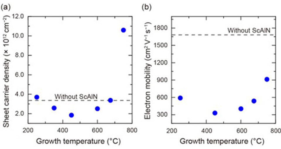
Image title: Variation of (a) sheet carrier density and (b) electron mobility of ScAlN/AlGaN/AlN/GaN heterostructures with growth temperature
Image caption: Growth temperature is a critical parameter determining the sheet carrier density of scandium aluminum nitride (ScAlN)-based heterostructures, grown using the sputtering technique.
Image credit: Dr. Atsushi Kobayashi from Tokyo University of Science, Japan
License type: CC BY 4.0
Usage restrictions: Credit must be given to the creator.
Reference
| Title of original paper | : | Effect of growth temperature on the structural and electrical properties of sputter-epitaxial ScAlN on AlGaN/AlN/GaN heterostructures |
| Journal | : | APL Materials |
| DOI | : | 10.1063/5.0281540 |
About The Tokyo University of Science
Tokyo University of Science (TUS) is a well-known and respected university, and the largest science-specialized private research university in Japan, with four campuses in central Tokyo and its suburbs and in Hokkaido. Established in 1881, the university has continually contributed to Japan's development in science through inculcating the love for science in researchers, technicians, and educators.
With a mission of "Creating science and technology for the harmonious development of nature, human beings, and society," TUS has undertaken a wide range of research from basic to applied science. TUS has embraced a multidisciplinary approach to research and undertaken intensive study in some of today's most vital fields. TUS is a meritocracy where the best in science is recognized and nurtured. It is the only private university in Japan that has produced a Nobel Prize winner and the only private university in Asia to produce Nobel Prize winners within the natural sciences field.
■
Tokyo University of Science(About TUS)
![]()
About Associate Professor Atsushi Kobayashi
from Tokyo University of Science
Dr. Atsushi Kobayashi is currently an Associate Professor in the Department of Materials Science and Technology at Tokyo University of Science (TUS), Japan. He obtained his M.S. and Ph.D. degrees from The University of Tokyo in 2005 and 2007, respectively. He has published over 130 articles that have received more than 2,000 citations. At TUS, he also leads the Kobayashi lab, where his research focuses on thin-film materials. His broader research interests include semiconductors, material characterization, epitaxial growth, electronic device fabrication, and superconductors.
Laboratory website ![]()
Official TUS website ![]()
Funding information
This study was partially supported by JSPS KAKENHI Grant Number JP23KK009, Izumi Science and Technology Foundation, and Research Foundation for the Electrotechnology of Chubu.