2025.07.09 Wednesday
First Look at Defects in Single-Crystal Indium Gallium Zinc Oxide Could Fix Persistent Display Instability
Insights into atomic-scale defects may enable next-generation thin-film transistors for smartphones, televisions, and flexible electronics

Many displays found in smartphones and televisions rely on thin-film transistors (TFTs) made from indium gallium zinc oxide (IGZO) to control pixels. IGZO offers high transparency due to its large bandgap (the gap existing between the valence and conduction bands), high conductivity, and can operate even in an amorphous (non-crystalline) form, making it ideal for displays, flexible electronics, and solar cells. However, IGZO-based devices face long-term stability issues, such as negative bias illumination stress, where prolonged exposure to light and electrical stress shifts the voltage required to activate pixels. These instabilities are believed to stem from structural imperfections, which create additional electronic states―known as subgap states―that trap charge carriers and disrupt current flow.
Until recently, most studies on subgap states focused on amorphous IGZO, as sufficiently large single-crystal IGZO (sc-IGZO) samples were not available for analysis. However, the disordered nature of amorphous IGZO has made it difficult to pinpoint the exact causes of electronic instability.
Now, using a newly developed method for growing high-quality single crystals of IGZO, a team led by Professor Tomohiko Saitoh from the Department of Applied Physics, Tokyo University of Science (TUS), Japan, has provided the first detailed look at how atomic-scale defects influence the material's electronic properties. The findings published in Volume 126, Issue 24 of the journal Applied Physics Letters as an Editor's Pick on June 16, 2025, represent a major step toward understanding and mitigating the causes of instability in IGZO-based devices.
The study was a collaborative effort involving Dr. Goro Shibata from the Department of Applied Physics (currently at the Japan Atomic Energy Agency), Professor Nobuaki Miyakawa from the Department of Applied Physics, TUS, and Dr. Akira Yasui from the Japan Synchrotron Radiation Research Institute.
"Studying the electronic structure of bulk IGZO single crystals helps us understand how the material's crystallinity impacts subgap states and what causes its anisotropic electrical conductivity," says Prof. Saitoh.
Using a recently developed optical floating zone method, the team successfully grew millimeter-sized single crystals of InGaZnO4 (IGZO-11). They prepared two types of samples: one in its as-grown state, containing natural oxygen vacancies, and another that was annealed―heated to 1,000 °C in an oxygen-rich environment―to eliminate these vacancies. They investigated the formation of subgap states near the valence and conduction bands of the material using hard X-ray photoemission spectroscopy (HAXPES)―a technique that uses high-energy photons to probe deep into materials and precisely map their electronic structure. HAXPES measurements were performed at the beamlines BL09XU and BL47XU of SPring-8, Japan.
In the as-grown crystals, the researchers detected irregularities in the core-level electron spectra, especially around indium atoms. In contrast, the annealed crystals showed smoother, more symmetrical signals. These asymmetries in the as-grown crystal indicated an uneven atomic environment due to nearby oxygen vacancies, which disappeared after annealing. The defects also appeared to cluster around indium atoms, suggesting that oxygen vacancies form more readily in the InO2 layers of the crystal.
The researchers found two types of oxygen bonding: metal-oxygen bonds and hydroxy (-OH) groups. The hydroxy bonds persisted even after annealing, indicating that they were not surface contaminants. Instead, they likely originated from trace water present during crystal growth, implying that such features are intrinsic to the material.
The most striking findings came from examining the material's energy bands. In the as-grown sample, the team detected extra electronic states just below the conduction band. However, no subgap states were found near the valence band in either the as-grown or annealed crystals. This stands in sharp contrast to amorphous IGZO, where such states are frequently observed and strongly linked to device instability. Their absence in the crystalline samples suggests these defects result not only from oxygen vacancies but also from structural disorder.
"The so-called subgap state just above the valence band was hardly observed in either as- grown or annealed samples, and we concluded that the formation of the subgap state is related to crystallinity, such as single crystal or amorphous," says Prof. Saitoh.
These results provide the first detailed insights into how atomic-scale defects and structural order influence the electronic properties of single-crystal IGZO. This research aids in two ways: determining the optimum annealing conditions in sample growing or identifying a sister material that possesses a homologous structure for the development of robust TFTs. By understanding how oxygen vacancies and structural order influence IGZO behavior, the findings can lead to more reliable and durable display technologies.
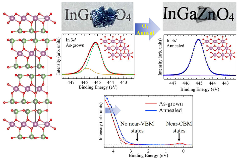
Image title: Atomic-scale defects and subgap formation in single-crystal IGZO (InGaZnO4)
Image caption: Using hard X-ray photoemission spectroscopy, researchers revealed how oxygen vacancies and structural disorder influence subgap state formation. The figure shows the InGaZnO4 crystal structure, the reduction of oxygen vacancies after annealing, and the presence of subgap states near the conduction band in the as-grown sample.
Image credit: Prof. Tomohiko Saitoh from Tokyo University of Science, Japan
License type: CC BY-NC 4.0
Usage restrictions: Credit must be given to the creator. Only non-commercial uses of the work are permitted.
Reference
| Title of original paper | : | Hard x-ray photoemission study of bulk single-crystalline InGaZnO4 |
| Journal | : | Applied Physics Letters |
| DOI | : | 10.1063/5.0271655 |
About The Tokyo University of Science
Tokyo University of Science (TUS) is a well-known and respected university, and the largest science-specialized private research university in Japan, with four campuses in central Tokyo and its suburbs and in Hokkaido. Established in 1881, the university has continually contributed to Japan's development in science through inculcating the love for science in researchers, technicians, and educators.
With a mission of "Creating science and technology for the harmonious development of nature, human beings, and society," TUS has undertaken a wide range of research from basic to applied science. TUS has embraced a multidisciplinary approach to research and undertaken intensive study in some of today's most vital fields. TUS is a meritocracy where the best in science is recognized and nurtured. It is the only private university in Japan that has produced a Nobel Prize winner and the only private university in Asia to produce Nobel Prize winners within the natural sciences field.
■
Tokyo University of Science(About TUS)
![]()
About Professor Tomohiko Saitoh
from Tokyo University of Science
Dr. Tomohiko Saitoh is a Professor in the Department of Applied Physics at Tokyo University of Science, where he specializes in condensed matter physics, photoemission spectroscopy, and the electronic structure of complex materials. He earned his Ph.D. in Physics from the University of Tokyo and has held research positions at the University of Colorado and KEK. Prof. Saitoh has authored over 100 peer-reviewed publications, including 81 refereed papers, and was recognized as an Outstanding Referee by the American Physical Society.
Laboratory website ![]()
Official TUS website ![]()
About Professor Nobuaki Miyakawa
from Tokyo University of Science
Funding information
This work was supported by JSPS KAKENHI Grant Nos. 17K05502 and 21K04909. The synchrotron radiation experiments at SPring-8 were performed under the approval of the Japan Synchrotron Radiation Research Institute (2018A1013, 2018B1049, 2018B1025, 2019A1433, 2019B1013, 2020A1258, 2020A1008, 2021A1415, 2021B1029, and 2021B1457).