2022.09.28 Wednesday
Scalable and Fully Coupled Quantum-inspired Processor Solves Optimization Problems
Researchers experimentally demonstrate the first fully connected annealing processor that can be scaled up across multiple chips
Annealing processors are more energy efficient and quicker at solving mathematical optimization problems than PCs. Researchers at Tokyo University of Science have now developed a new approach to realizing scalable fully coupled annealing processors. These quantum-inspired systems can model the interactions between magnetic spins and use it to solve complex optimization problems. The new method greatly outperforms modern CPUs and shows potential for applications in drug discovery, artificial intelligence, and materials science.
Have you ever been faced with a problem where you had to find an optimal solution out of many possible options, such as finding the quickest route to a certain place, considering both distance and traffic? If so, the problem you were dealing with is what is formally known as a "combinatorial optimization problem." While mathematically formulated, these problems are common in the real world and spring up across several fields, including logistics, network routing, machine learning, and materials science.
However, large-scale combinatorial optimization problems are very computationally intensive to solve using standard computers, making researchers turn to other approaches. One such approach is based on the "Ising model," which mathematically represents the magnetic orientation of atoms, or "spins," in a ferromagnetic material. At high temperatures, these atomic spins are oriented randomly. But as the temperature decreases, the spins line up to reach the minimum energy state where the orientation of each spin depends on its neighbors. It turns out that this process, known as "annealing," can be used to model combinatorial optimization problems such that the final state of the spins yields the optimal solution.
Researchers have tried creating annealing processors that mimic the behavior of spins using quantum devices, and have attempted to develop semiconductor devices using large-scale integration (LSI) technology aiming to do the same. In particular, Professor Takayuki Kawahara's research group at Tokyo University of Science (TUS) in Japan has been making important breakthroughs in this particular field.
In 2020, Prof. Kawahara and his colleagues presented at the 2020 international conference, IEEE SAMI 2020, one of the first fully coupled (that is, accounting for all possible spin-spin interactions instead of interactions with only neighboring spins) LSI annealing processors, comprising 512 fully-connected spins. Their work appeared in the journal IEEE Transactions on Circuits and Systems I: Regular Papers. These systems are notoriously hard to implement and upscale owing to the sheer number of connections between spins that needs to be considered. While using multiple fully connected chips in parallel was a potential solution to the scalability problem, this made the required number of interconnections (wires) between chips prohibitively large.
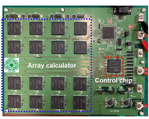
In a recent study published in Microprocessors and Microsystems, Prof. Kawahara and his colleague demonstrated a clever solution to this problem. They developed a new method in which the calculation of the system's energy state is divided among multiple fully coupled chips first, forming an "array calculator." A second type of chip, called "control chip," then collects the results from the rest of the chips and computes the total energy, which is used to update the values of the simulated spins. "The advantage of our approach is that the amount of data transmitted between the chips is extremely small," explains Prof. Kawahara. "Although its principle is simple, this method allows us to realize a scalable, fully connected LSI system for solving combinatorial optimization problems through simulated annealing."
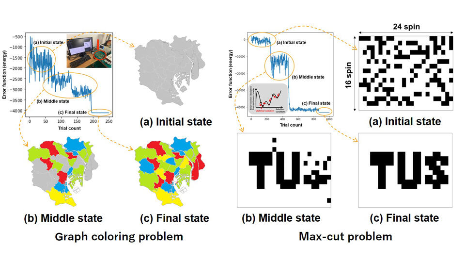
The researchers successfully implemented their approach using commercial FPGA chips, which are widely used programmable semiconductor devices. They built a fully connected annealing system with 384 spins and used it to solve several optimization problems, including a 92-node graph coloring problem and a 384-node maximum cut problem. Most importantly, these proof-of-concept experiments showed that the proposed method brings true performance benefits. Compared with a standard modern CPU modeling the same annealing system, the FPGA implementation was 584 faster and 46 times more energy efficient when solving the maximum cut problem.
Now, with this successful demonstration of the operating principle of their method in FPGA, the researchers plan to take it to the next level. "We wish to produce a custom-designed LSI chip to increase the capacity and greatly improve the performance and power efficiency of our method," Prof. Kawahara remarks. "This will enable us to realize the performance required in the fields of material development and drug discovery, which involve very complex optimization problems."
Finally, Prof. Kawahara notes that he wishes to promote the implementation of their results to solve real problems in society. His group hopes to engage in joint research with companies and bring their approach to the core of semiconductor design technology, opening doors to the revival of semiconductors in Japan.
Make sure to watch out for these groundbreaking annealing processors in the future!
|
|
Image title: Solving combinatorial optimization problems with a scalable fully coupled annealing processor.
Image caption: In a new study, researchers from TUS, Japan, proposed a fully connected scalable annealing processor that, when implemented in FPGA, can easily outperform a modern CPU in solving various combinatorial optimization problems in terms of speed and energy consumption. The proposed method achieves this using an "array calculator," consisting of multiple coupled chips, and a "control chip." It could be applied to solve similar complex optimization problems in logistics, network routing, warehouse management, personnel assignment, drug delivery, and materials science.
Image credit: Takayuki Kawahara from TUS, Japan
License type: Original content
Usage restrictions: Cannot be reused without permission
Reference
| Title of original paper | : | Scalable Fully Coupled Annealing Processing System and Multi-chip FPGA Implementation |
| Journal | : | Microprocessors and Microsystems |
| DOI | : | 10.1016/j.micpro.2022.104674 |
| Title of related paper | : | Annealing Processing Architecture of 28-nm CMOS Chip for Ising Model With 512 Fully-coupled Spins |
| Journal | : | IEEE Transactions on Circuits and Systems I: Regular Papers |
| DOI | : | 10.1109/TCSI.2021.3114422 |
About The Tokyo University of Science
Tokyo University of Science (TUS) is a well-known and respected university, and the largest science-specialized private research university in Japan, with four campuses in central Tokyo and its suburbs and in Hokkaido. Established in 1881, the university has continually contributed to Japan's development in science through inculcating the love for science in researchers, technicians, and educators.
With a mission of "Creating science and technology for the harmonious development of nature, human beings, and society", TUS has undertaken a wide range of research from basic to applied science. TUS has embraced a multidisciplinary approach to research and undertaken intensive study in some of today's most vital fields. TUS is a meritocracy where the best in science is recognized and nurtured. It is the only private university in Japan that has produced a Nobel Prize winner and the only private university in Asia to produce Nobel Prize winners within the natural sciences field.
About Professor Takayuki Kawahara from Tokyo University of Science
Prof. Takayuki Kawahara obtained his BS, MS, and PhD degrees from Kyushu University, Japan. With his MS degree, he joined Hitachi Central Research Laboratory as a research staff member. After leaving the laboratory as a Chief Researcher, he joined the Tokyo University of Science in 2014 to work on developing sustainable electronics. His research group carries out cutting-edge research in the field of ultra-low-power AI devices, circuits, and systems. With more than 160 publications to his credit, Prof. Kawahara has won numerous international awards, including the prizes for Science and Technology, Development Category, awarded by the Ministry of Education, Culture, Sports, Science and Technology.
Funding information
This study was partially supported by JSPS KAKENHI Grant Number 22H01559.