2022.01.13 Thursday
Towards High-performance Organic Optoelectronics with Better Crystallinity at Semiconductor Interface
Organic molecular interfaces with minimized structural mismatch and spontaneous electron transfer could open doors to high-efficiency optoelectronics
Organic semiconductors have garnered much attention in optoelectronics owing to their flexibility, which is allowed by weak interaction forces. However, this also makes for poor charge carrier mobility. In a new study, researchers from Japan combined organic semiconductor molecules with similar structures to produce interfaces with better crystal quality and charge transport efficiency, paving the way for the realization of high-mobility organic optoelectronics.
|
Semiconductor electronic devices can be made of either inorganic crystals, formed by the strong bonding of atoms and ions, or organic crystals, which demonstrate weaker bonds held together by van der Waals forces (weak electric forces of attraction between neutral atoms or molecules that do not share a chemical bond). These weak bonds make organic semiconductors viable for flexible optoelectronics applications such as wearable electronic devices and flexible solar cells. However, this very characteristic also lends them a disadvantage: organic semiconductors typically exhibit poor charge carrier mobility and, therefore, do not conduct electricity well.
It is well-known that single-crystalline semiconductors can conduct electricity much better compared to their non-crystalline forms. Moreover, crystals composed of organic molecules can be grown to have interfaces with little structural mismatch even when their structures are quite different. Is there a way to leverage these properties to improve the charge transport in organic semiconductors?
This is where researchers from Tokyo University of Science, Japan decided to step in. In a new study led by Associate Professor Yasuo Nakayama, the researchers attempted to enhance the charge transport efficiency by minimizing the crystal structure mismatch between the growing crystal layer and the substrate. "I wanted to confirm whether the quality of the crystals at the interface would be better if we combined materials with similar structures so that we could create a crystalline interface even with inorganic materials," says Dr. Nakayama, speaking of his personal motivation for the research. The paper was made available online on 18 November 2021, and published in Volume 12, Issue 46 of The Journal of Physical Chemistry Letters on 25 November 2021.
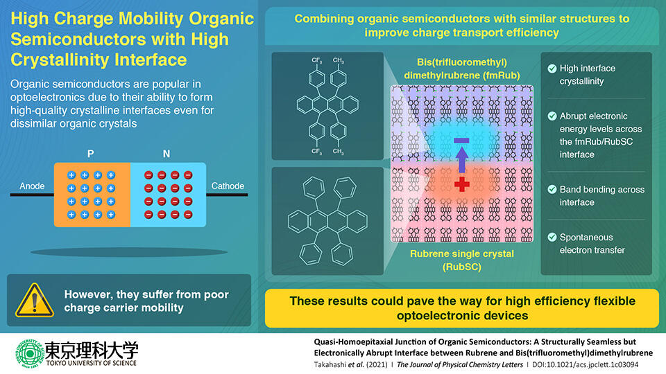
The team designed a high-quality crystalline interface using a technique called "quasi-homo-epitaxial growth" to grow bis(trifluoromethyl)dimethylrubrene on a single crystal surface of rubrene. They used surface X-ray diffraction measurements to characterize the interface and demonstrated its high crystallinity resulting from minimized structure mismatch. This eliminated the mobility issue. Additionally, they probed its electronic structure using ultraviolet photoelectron spectroscopy, which revealed an abrupt step in the electronic energy levels across the interface. This allowed for spontaneous electron transfer across the interface, validating their strategy.
With these results, the team is now excited about the potential applications their findings could entail. "Our work could potentially open up an untested route for the realization of high-mobility organic semiconductor optoelectronics. Additionally, since organic semiconductors can be made into thin and light crystals, it is possible to print semiconductor devices on transparent films and fabrics for carrying and wearing," speculates Dr. Nakayama. "Furthermore, it could also lead to highly efficient flexible solar cells with better performance than those of existing technologies."
Those certainly are some fascinating consequences to look forward to!
Reference
| Title of original paper | : | Quasi-Homoepitaxial Junction of Organic Semiconductors: A Structurally Seamless but Electronically Abrupt Interface between Rubrene and Bis(trifluoromethyl)dimethylrubrene |
| Journal | : | The Journal of Physical Chemistry Letters |
| DOI | : | 10.1021/acs.jpclett.1c03094 |
About The Tokyo University of Science
Tokyo University of Science (TUS) is a well-known and respected university, and the largest science-specialized private research university in Japan, with four campuses in central Tokyo and its suburbs and in Hokkaido. Established in 1881, the university has continually contributed to Japan's development in science through inculcating the love for science in researchers, technicians, and educators.
With a mission of "Creating science and technology for the harmonious development of nature, human beings, and society", TUS has undertaken a wide range of research from basic to applied science. TUS has embraced a multidisciplinary approach to research and undertaken intensive study in some of today's most vital fields. TUS is a meritocracy where the best in science is recognized and nurtured. It is the only private university in Japan that has produced a Nobel Prize winner and the only private university in Asia to produce Nobel Prize winners within the natural sciences field.
About Associate Professor Yasuo Nakayama from Tokyo University of Science
Dr. Yasuo Nakayama is an Associate Professor at the Department of Pure and Applied Chemistry at TUS. In 2005, he obtained his doctorate degree from The University of Tokyo, Japan, following which he joined there at the Department of Physics. His main research interest lie in device related chemistry, organic semiconductors, electronic structure, photoelectron spectroscopy, and surface science. He has 89 publications to his name and has won multiple awards for his research.
https://www.tus.ac.jp/en/fac/p/index.php?6b37 ![]()
https://www.rs.tus.ac.jp/oml/index.html ![]()
Funding information
This study was supported by Nanotechnology Platform Programs "Molecule and Material Synthesis" (JPMXP09S19MS0018, JPMXP09S20MS0007, and JPMXP09S21MS0010) of the Ministry of Education, Culture, Sports, Science and Technology (MEXT), Japan, by the JSPS-KAKENHI [JP21H05405 and JP21H05411] and the Futaba Foundation, and by JST PRESTO (JPMJPR2101).