| 紹介 |
物理世界の(アナログ)情報と、クラウド等にて扱うデジタルビットの情報とを、AIも活用して賢くつなぐ部分の拡張・深堀を進めています。素子・回路・システムの各階層にて新たな原理も探求しながら多様な処理を高速かつ低電力にて行います。サステナブル社会を支えるエレクトロニクスの研究です。(2014.4)
2025年10月より文部科学省「半導体人材育成拠点形成事業」の未来共創半導体イノベーションアリーナ(SiCA)において産学連携統括。2026年4月よりTUS SciTech半導体共創教育研究センター(TUS SciTech SCoRE Center) センター長。
TUS SciTech半導体共創教育研究センター(TUS SciTech SCoRE Center):
半導体関連分野および集積回路を中心として様々な分野への展開ならびにこれらの分野の教育と研究に関して、学内外と共創して推進する。半導体のさらなる応用を思考可能な、ならびに半導体の設計可能な実力のある人材を育成するとともに、産学官の連携により研究を発展させ、世界的な研究拠点を形成できるように活動する。
TUS SciTech Semiconductor Co-Creation Research and Education Center (TUS SciTech SCoRE Center):
The TUS SciTech Semiconductor Co-Creation Research and Education Center (TUS SciTech SCoRE Center) is a hub for semiconductor education, research, and industry–academia collaboration established by Tokyo University of Science under the TUS SciTech Initiative.
The Center develops the next generation of semiconductor professionals through the MEXT-supported SiCA program and collaborates with national initiatives in advanced semiconductor research and development, including LSTC. By bringing together education, research, and industry–academia–government collaboration, the Center aims to contribute to the future of semiconductor technology and industry.
Mission
Our mission is to advance semiconductor education and research through co-creation across disciplines and sectors.
We foster professionals who can not only design semiconductor devices and integrated circuits, but also envision new applications of semiconductor technologies. Through close collaboration among academia, industry, and government, we pursue innovative research and aim to build a globally connected hub for semiconductor education and research.
|
| 研究テーマ |
-
東京理科大学工学部電気工学科(定員110名)3年生必修科目学生実験テーマに全結合型イジングマシンLSI実装
継続的かつ系統的な研究成果を踏まえ、2025年度から東京理科大学工学部電気工学科3年生の必修科目である学生実験に、全結合型イジングマシンのLSI実装を組み込みました。
実験テーマの1つとして、基本的な全結合型イジングマシンのFPGA実装および評価を行う内容です。今後、電気工学科3年生全員が、全結合型イジングマシンという1つのまとまった機能を実現する集積回路をFPGAを用いて設計・実装し、LSIハードウエアとして動作させます。これは近年、強化が求められている半導体設計技術の良い学びの機会となります。実験の内容については、公開されているシラバスで確認できます。
Starting in 2025, an LSI implementation of a fully coupled Ising machine was incorporated into student experiments, a required subject for third-year students in the Department of Electrical Engineering, Faculty of Engineering, Tokyo University of Science.
-
2026年度未来共創半導体イノベーションアリーナ(SiCA)推奨科目の開講
文部科学省「半導体人材育成拠点形成事業(enSET)」の「未来共創半導体イノベーションアリーナ(SiCA:シーカ)」に連携校として参加しています。2026年度本事業の一環として大学院修士課程向けのSiCA推奨科目を開講します。
-
TUS SciTech Semiconductor Co-Creation Research and Education Center (TUS SciTech SCoRE Center)
The TUS SciTech Semiconductor Co-Creation Research and Education Center (TUS SciTech SCoRE Center) is a hub for semiconductor education, research, and industry–academia collaboration established by Tokyo University of Science under the TUS SciTech Initiative.
The Center develops the next generation of semiconductor professionals through the MEXT-supported SiCA program and collaborates with national initiatives in advanced semiconductor research and development, including LSTC. By bringing together education, research, and industry–academia–government collaboration, the Center aims to contribute to the future of semiconductor technology and industry.
Mission
Our mission is to advance semiconductor education and research through co-creation across disciplines and sectors.
We foster professionals who can not only design semiconductor devices and integrated circuits, but also envision new applications of semiconductor technologies. Through close collaboration among academia, industry, and government, we pursue innovative research and aim to build a globally connected hub for semiconductor education and research.
-
半導体人材育成
文科省半導体人材育成事業SiCAに従事しております。
理科大は既に多くの半導体人材を輩出しています(HP掲載就職先一覧から下記)。
これを更に広げていきます。
2022.3~2026.3卒累計
ソニーセミコンダクタソリューションズ 72名
キオクシア 49名
東京エレクトロン 49名
-
書籍:『人工知能チップ回路入門』(コロナ社)
☆2024年9月4日、『人工知能チップ回路入門』(コロナ社)が出版されました。
☆成長基幹産業である半導体や集積回路に興味を持ち、発展が期待されるエッジ側での人工知能(AI)による情報処理に関心のある若手技術者・高専・大学の学生の皆さんへおすすめな、手頃なページ数のAIチップ入門書です。3つの面からの入門レベルの内容です。
☆1.(2章~4章):ニューラルネットワークの基本的な説明から始め、電子回路の基本も概説した上で、回路ブロックレベルで人工知能チップの構成。各種ニューラルネットワークとして、2024年ノーベル賞対象技術であるホップフィールドネットワークやボルツマンマシンにも初歩的に簡単にだが触れている。
☆2.(5章、6章):高性能化に重要であるニアメモリコンピューティング、インメモリコンピューティング技術。
☆3.(7章、8章):全結合型イジングマシン技術(ニューラルネットワークのひとつであるホップフィールドネットワーク(2024年ノーベル賞対象技術)+アニーリング機構)。

-
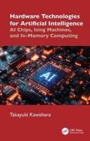
書籍2:『Hardware Technologies for Artificial Intelligence: AI Chips, Ising Machines, and In-Memory Computing』(CRC Press)
☆2025年12月5日に出版されました。
☆次世代計算技術を体系的に解説した総合的な参考書です。
☆LSI設計とニューラルネットワークの基礎から大規模化・高効率化の手法を示し、AIチップ、イジングマシンLSI事例、インメモリコンピューティングでのAI計算基礎、及び将来展望を解説しています。
☆学生から研究者・技術者まで、次世代計算の方向性を理解し応用できる内容となっています。
-
科学技術分野の文部科学大臣表彰
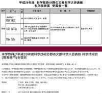
東京理科大学の推薦によって、平成29年度(2017年度)の文部科学大臣表彰を頂きました。
竹村理一郎氏(日立製作所)、大野英男氏(東北大学)との共同受賞によるものであり、スピン注入磁化反転メモリ(STT-RAM)の大容量化をめざした「STT-RAM大容量化回路技術に関する先駆的研究開発」に関する業績が高く評価されました。STT-RAMは、高速性、低消費電力、高耐久性を兼ね備えしかも宇宙線に強いメモリ技術であり、現在では多くの製品化が進んでいます(応用先用途:ウエアラブル端末、産業用マイコン、車載用マイコン、人工知能エッジ端末)。その礎となった研究開発です。
平成29年度 科学技術分野の文部科学大臣表彰 科学技術賞(開発部門)
受賞者:河原尊之(東京理科大学)、竹村理一郎(日立製作所)、大野英男(東北大学)
業績名:STT-RAM大容量化回路技術に関する先駆的研究開発
推薦機関:東京理科大学
文科省(平成29年度 科学技術分野の文部科学大臣表彰 科学技術賞 受賞者一覧):
https://www.mext.go.jp/b_menu/houdou/29/04/__icsFiles/afieldfile/2017/04/11/1384228_01.pdf
理科大プレスリリース(英文):
https://www.tus.ac.jp/en/news/archive/20170419001.html
(共にリンクはしていないのでコピーされてお使いください)
-
TUS Faculty Receives FY2017 Commendation for Science and Technology by the MEXT Prize for Science and Technology (Development Category)
Professor Takayuki Kawahara of the Department of Electrical Engineering in the Faculty of Engineering at TUS, Riichiro Takemura (Hitachi, Ltd.), and Hideo Ono (Tohoku University) have been awarded the FY2017 Commendation for Science and Technology by the Minister of Education, Culture, Sports, Science and Technology Prize for Science and Technology (Development Category).
The award for Science and Technology (Development Category) is given to individuals and groups who have made revolutionary research and development or an invention that contributes to the development of the socioeconomics and the life of the people in Japan, and that is actually being utilized, or to individuals who have fostered such persons.
Professor Kawahara et al. have utilized the refinement potential of the STT method (rewriting with spin polarized current) and were the first to develop a circuit technology for necessary memory (RAM). They were highly regarded for opening up a path to commercialization of large capacity, nonvolatile RAM. The technology that they developed became the standard for subsequent research and development throughout the world.
These research results will contribute to significant power saving of IoT/mobile devices, computers, and deep learning, and broadly to artificial intelligence (AI) servers as well.
https://www.tus.ac.jp/en/news/archive/20170419001.html
-
全結合型イジング半導体システム
社会の至る所で課題となる組合せ最適化問題を解く"全結合型"イジングマシンは、ニューラルネットワークのひとつであるホップフィールドネットワーク(2024年ノーベル賞対象技術の一つ)+アニーリング機構。この全結合型イジングマシンのLSI実装を検討。
2020年;一次元スピン配列と二次元スピン間相互作用配列を用いて計算されたエネルギーに基づいてスピンの値を更新する全結合アニーリングプロセッサのLSI実装のためのアーキテクチャ(NEDO先導調査研究2018-19)
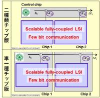
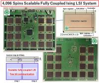
2022年(FPGA)、2024年(LSIシステム):チップ間接続本数で複数の全結合イジングLSIチップを全結合のまま結合でき、全体でひとつの全結合システムとして動作する大規模イジングLSIシステムをスケーラブルに構成するアーキテクチャ。規模(容量)と精度の両方でスケーラブル化が可能となる画期的な構成(下図。特許出願済。科研費22H01559、科研費23K22829、科研費25K07849)
-
4,096 Spins Scalable Fully Coupled Ising LSI System (Hopfield Network + Annealing mechanism)
A fully coupled Ising system is a Hopfield network (one of the technologies eligible for the 2024 Nobel Prize). It includes an annealing mechanism. Toward the realization of a large-scale fully-coupled Ising semiconductor system, we have successfully verified a scalable technology using multiple LSI chips, setting a target for large capacity expansion.
This time, a scalable 4,096-spin fully-coupled Ising processing system was realized using 36 22nm CMOS computation LSI chips and a control FPGA.
Compared to an annealing emulation that mimics a fully connected Ising system on a PC, we achieved a 2,306-fold increase in performance, and a 2,186-fold increase in core units (CPU and computation chip).
本研究の一部は、日本学術振興会科学研究費補助金(課題番号 22H01559, 23K22829, 25K07849)の助成を受けて実施したものです。
-
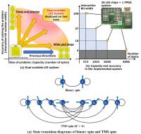
Dual Scalable Ising LSI System and multi-state structure
1. We developed an innovative dual scalable annealing processing (AP) system (DSAPS) that can simultaneously scale both ”capacity” and ”precision” using the same scalable structure. DSAPS achieves dual scalability by manipulating ∆E blocks, responsible for computing the energy of the system, using two structures. i.e., the conventional high-capacity structure and a novel high-precision structure. Each ∆E block is equivalent to a large-scale integrated (LSI) chip on a CMOS-based AP board and includes the interaction matrix and the spins.
2. APs that have fully-coupled spin coupling are the focus of active research due to their ability to handle a wide range of Combinatorial Optimization Problems. However, since a single spin is updated by referring to the states of all other spins, sequential spin updates are necessary. This makes it difficult to achieve both high computation time and stable solution quality. Here, we propose transition-based multi-state pseudo annealing (TMSPA), which is an annealing method that allows discrete spin states between and maps the conventional two spin states to different transition directions.
本研究の一部は、日本学術振興会科学研究費補助金(課題番号 23K22829, 25K07849)の助成を受けて実施したものです。
-
Fully coupled Ising machine capable of simultaneous all-spin updates using multi-state spins
Fully coupled Ising machines are capable of handling a wide range of combinatorial optimization problems. However, because each spin is updated by referencing the states of all other spins, the spins must be updated sequentially. Consequently, it has been difficult to simultaneously achieve fast computation and stable solution quality.
To address this challenge, we have developed a new annealing method that enables the "simultaneous update of all spins" by employing multi-state spins instead of conventional binary spins, thereby solving combinatorial optimization problems quickly and stably. This approach is exceptionally effective in optimization domains that demand high speed, parallelism, and large-scale processing. The multi-state spins increase the search degrees of freedom and allow for the simultaneous updating of all spins, resulting in a structure well-suited for hardware implementation.
The technical details of this work were presented at IEEE SmartIoT 2025, an international conference held in Sydney, and the full paper has been published in IEEE Access.
本研究の一部は、日本学術振興会科学研究費補助金(課題番号25K07849)の助成を受けて実施したものです。:
-
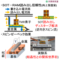
スピン流応用(SOT-RAM:科研費19K04536)
①Yuwa Kishi, Akihiro Yamada, Mengnan Ke, Takayuki Kawahara, "
Evaluation of Read Disturbance Reduction Effect by SOT-MRAM Bi-directional Read on Device Size Dependence" IEEE Intermag 2021 (2021.4)、②Yuwa Kishi, Keisuke Tabata, Mengnan Ke, Takayuki Kawahara, "Evaluation of Read Disturbance Reduction Effect by Bi-directional Read on Ferromagnetic Material Properties of SOT-MRAM," IEEE MMM 2020 (2020.11)、③Y. Kishi, M. Ke, M. Itoh, R. Kashiwa, T. Matsuzaki, T. Kawahara , "Impact of the metal/YIG interfaces in Pt/(W)/Y3Fe5O12/Gd3Ga5O12 and W/Y3Fe5O12/Gd3Ga5O12 structures for spin Seebeck effect," IEEE Intermag 2020 (2020.5)、④Atsushi Yamamoto, Takayuki Kawahara, "Evaluation of Spin Seebeck Effect in Single-crystal and Polycrystal Y3Fe5O12 (YIG)," IEEE MMM-Intermag (2019.1)、⑤Atsushi Yamamoto, Makoto Arai, Tetsuya Takimoto, Masatoshi Itoh, Takayuki Kawahara, "Evaluation of Correlation between Orientation of Y3Fe5O12 (YIG) Thin Film and Spin Seebeck Effect," 応用物理学会春季学術講演(2018.3)、⑥Atsushi Yamamoto, Makoto Arai, Tetsuya Takimoto, Masatoshi Itoh, Shizutoshi Ando, Shigeru Saito, Takayuki Kawahara, "Evaluation of Correlation Between Orientation of Y3Fe5O12(YIG) Thin Film and Spin Seebeck Effect," IEEE Intermag (2017.4)、⑧Hirokazu Kazama, Takayuki Kawahara, "Spin-Orbit Torque MRAM Read Reliability," IEEE Intermag
|